The semiconductor industry stands as the cornerstone of global technological advancement, driving innovations in computing, communication, and smart devices. As semiconductor components continue to shrink—with process nodes advancing to 3nm and beyond—manufacturing and inspection processes demand unprecedented precision. Even a micron-level deviation or a tiny defect can render a semiconductor chip non-functional, leading to massive production losses. Among the critical tools enabling this precision is the telecentric lens—a specialized industrial lens that eliminates perspective errors and ensures consistent magnification across the entire field of view (FOV), making it indispensable for semiconductor inspection tasks.
A leading provider of high-performance telecentric lenses tailored to semiconductor industry needs is Yixian Sensor Technology Co., Ltd. (Yixian Sensor). Its Telecentric Lens Series, designed with ultra-low distortion, high resolution, and excellent depth of field (DOF), addresses the unique challenges of semiconductor manufacturing—from wafer edge inspection to chip packaging verification. For detailed specifications, application cases, and technical support related to Yixian Sensor’s telecentric lenses and other semiconductor-focused optical solutions, visit its official product page: https://www.yixiansensor.com/en_US/products. Yixian Sensor’s telecentric lenses not only meet the semiconductor industry’s strict quality standards but also adapt to the high-speed, high-stability demands of 24/7 semiconductor production lines.
The semiconductor manufacturing process—spanning wafer fabrication, chip packaging, and final testing—involves diverse components and intricate steps, each requiring specialized optical inspection. Below are the four most critical application scenarios where telecentric lenses excel, paired with Yixian Sensor’s targeted solutions.
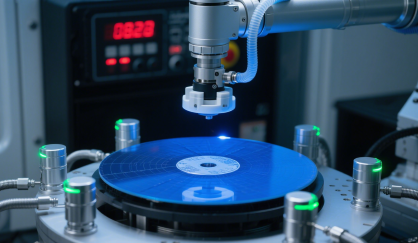
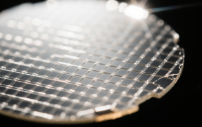
Wafers, the base material for semiconductor chips, undergo multiple processes such as photolithography, etching, and deposition. Even minor defects like scratches, particle contamination, or pattern misalignment on the wafer surface can ruin thousands of chips. Telecentric lenses here are essential for accurate defect detection and pattern dimension measurement due to their non-perspective imaging 特性.
• Wafer Edge Inspection: The edge of a wafer (typically 8-inch or 12-inch in diameter) is prone to chipping or coating unevenness, which can cause particle shedding and contaminate the manufacturing environment. Yixian Sensor’s Low-Distortion Telecentric Lens Series (available on its product page) features a distortion rate of < 0.03%, capturing uniform images of the wafer edge. This enables machine vision systems to detect tiny chips (as small as 5μm) and uneven coating, preventing defect propagation to the wafer’s active area.
• Photolithography Pattern Alignment: During photolithography, circuit patterns are transferred onto the wafer with nanoscale precision. A misalignment of just a few nanometers can lead to pattern overlap and chip failure. Yixian’s High-Resolution Telecentric Lens, compatible with 80MP high-sensitivity cameras, resolves fine circuit patterns (down to 0.1μm line width) and ensures accurate alignment measurement. Its large DOF (up to 5mm) allows simultaneous focusing on the wafer surface and pattern edges, eliminating refocusing delays in high-speed photolithography lines.
• Particle Contamination Detection: Tiny particles (≥0.5μm) on the wafer surface can cause short circuits in chip circuits. Yixian Sensor’s Coaxial Illumination Telecentric Lens integrates coaxial light sources to suppress surface glare, clearly visualizing even transparent or reflective particles. This is critical for maintaining the cleanliness of the wafer during fabrication, as particle contamination is one of the leading causes of wafer yield loss.
Chip packaging involves bonding the semiconductor die to a substrate, connecting them with thin wires, and encapsulating the assembly to protect against external factors. This stage requires micron-level alignment accuracy and reliable defect detection of bonding wires and encapsulation materials—tasks where telecentric lenses’ perspective-free imaging is irreplaceable.
• Die Bonding Alignment: The semiconductor die (as small as 1mm × 1mm for some microchips) must be bonded to the substrate with ±1μm accuracy. Yixian Sensor’s Dual-Telecentric Lens (a specialized type in its Telecentric Lens Series) captures images of both the die and substrate simultaneously without perspective distortion. This ensures the die is placed exactly at the target position, avoiding bonding errors that could lead to poor electrical connectivity.
• Wire Bond Inspection: Ultra-thin gold or copper wires (diameter 10μm–20μm) connect the die to the package pins. Defects like wire breakage, irregular loop height, or poor pin bonding can cause chip failure. Yixian’s High-Speed Telecentric Lens supports frame rates up to 200fps, capturing real-time images of wire bonds. Its high contrast imaging capability clearly distinguishes wires from the substrate background, enabling machine vision systems to detect even subtle wire shape deviations—critical for high-density chip packaging (e.g., BGA, QFP packages).
• Encapsulation Defect Detection: After wire bonding, the chip is encapsulated with epoxy resin to protect against moisture and vibration. Bubbles, cracks, or uneven encapsulation on the surface can compromise chip reliability. Yixian Sensor’s Wide-FOV Telecentric Lens covers the entire encapsulation area of large chips (e.g., CPU or GPU packages) in a single shot, detecting bubbles as small as 10μm and cracks as thin as 2μm. Its uniform imaging ensures no defects are missed due to perspective-related size variations.
Semiconductor components such as microchips, sensors, and MEMS (Micro-Electro-Mechanical Systems) have complex 3D structures and ultra-small dimensions. Accurate measurement of these dimensions—such as die thickness, pin pitch, and sensor cavity depth—is critical for ensuring compatibility with downstream assembly. Telecentric lenses enable accurate 2D and 3D dimension measurement by eliminating size variations caused by object distance.
• Die Thickness Measurement: The thickness of a semiconductor die (typically 50μm–500μm) must be measured with ±0.5μm accuracy to ensure proper packaging. Yixian Sensor’s Telecentric Lens with Laser Triangulation Compatibility pairs with laser displacement sensors to capture 3D depth data of the die. This allows precise measurement of thickness variations across the die surface, preventing packaging issues like uneven pressure on the die.
• Pin Pitch Measurement: Semiconductor packages (e.g., QFP, LGA) have pins with pitches as small as 0.4mm. Even a 0.05mm deviation in pin pitch can cause poor soldering to PCBs. Yixian’s High-Precision Telecentric Lens ensures consistent magnification across the entire FOV, enabling accurate measurement of pin pitch and pin height. Its MTF (Modulation Transfer Function) value of > 0.8 at 200 lp/mm ensures clear edge definition of tiny pins, reducing measurement errors to < 0.01mm.
• MEMS Sensor Cavity Measurement: MEMS sensors (e.g., accelerometers, gyroscopes) have tiny internal cavities (depth 1μm–10μm) that affect their performance. Yixian Sensor’s Ultra-High-Resolution Telecentric Lens resolves these micro-cavities, enabling machine vision systems to measure cavity depth and shape with high accuracy. This is essential for ensuring the sensitivity and reliability of MEMS sensors used in smartphones, wearables, and automotive electronics.
After manufacturing, semiconductor chips undergo rigorous testing to ensure they meet performance specifications. This includes functional testing, voltage testing, and 外观 inspection. Telecentric lenses play a key role in final 外观 defect detection and testing fixture alignment, ensuring only qualified chips enter the market.
• Final 外观 Defect Detection: Chips with surface scratches, paint peeling, or logo misalignment are considered defective. Yixian Sensor’s Polarized Telecentric Lens suppresses glare from the chip’s reflective surface (e.g., metal pins, glass coatings), clearly visualizing even subtle scratches (as small as 3μm) and logo misalignment. This ensures no cosmetic defects are missed during final inspection.
• Testing Fixture Alignment: During functional testing, chips are connected to testing fixtures via probes. Accurate alignment of the chip with the probes (±2μm accuracy) is critical to avoid probe damage and ensure reliable test results. Yixian’s Dual-Telecentric Lens captures images of both the chip and probes simultaneously, enabling real-time alignment adjustment. Its non-perspective imaging ensures the relative position of the chip and probes is measured accurately, reducing test errors and improving testing efficiency.
The semiconductor industry imposes stricter requirements on telecentric lenses than other industries—demanding ultra-low distortion, high resolution, excellent environmental adaptability, and compatibility with high-speed production lines. Yixian Sensor’s telecentric lenses address these needs with three key advantages:
• Ultra-Low Distortion and High Resolution: Yixian’s telecentric lenses feature a distortion rate of < 0.03%, far lower than the industry average of 0.1%. They support 12MP–80MP cameras with MTF values > 0.8 at 200 lp/mm, enabling sub-micron detail resolution—critical for detecting tiny defects and measuring nanoscale semiconductor patterns.
• Excellent Environmental Adaptability: Semiconductor manufacturing environments require lenses to withstand cleanroom conditions, temperature fluctuations, and vibration. Yixian’s telecentric lenses undergo strict environmental testing, including 1,000-hour high-temperature (85°C) and low-temperature (-40°C) cycling tests, and 15G vibration tests. They also feature anti-static coatings (10^6–10^9 Ω) to prevent electrostatic damage to sensitive semiconductor components and dust-proof designs (IP67-rated) to meet cleanroom standards (Class 100).
• High-Speed and Easy Integration: Yixian’s telecentric lenses support frame rates up to 200fps, matching the speed of high-volume semiconductor production lines (e.g., 1,000 wafers per hour). Their standardized mechanical interfaces (e.g., C-mount, F-mount) and compatibility with mainstream machine vision cameras (e.g., Basler, Keyence) simplify system integration, reducing deployment time for semiconductor manufacturers.
As the semiconductor industry evolves toward smaller process nodes (e.g., 2nm and below), 3D IC packaging, and advanced MEMS devices, Yixian Sensor is advancing its telecentric lens portfolio to meet emerging needs:
• 3D IC Packaging Inspection: 3D IC packaging, which stacks multiple chips vertically, requires inspection of inter-chip connections (e.g., through-silicon vias, TSVs) with sub-micron accuracy. Yixian is developing 3D Telecentric Lenses that integrate structured light technology to capture 3D depth data of TSVs, enabling accurate measurement of via depth and alignment.
• Advanced MEMS Inspection: Next-gen MEMS devices (e.g., micro-robots, bio-sensors) have more complex 3D structures, requiring higher-resolution 3D inspection. Yixian is enhancing its telecentric lenses with higher magnification (up to 100x) and improved DOF (up to 10mm) to resolve intricate MEMS structures.
• AI-Driven Adaptive Inspection: Yixian is integrating AI algorithms into its telecentric lens systems to enable auto-adjustment of focus, magnification, and illumination based on the type of semiconductor component being inspected (e.g., wafer, chip, MEMS). This will eliminate manual parameter tuning, reducing human error and improving inspection efficiency.
Telecentric lenses are the "precision eyes" of the semiconductor industry, enabling the accurate inspection and measurement that is critical for high-yield, high-quality semiconductor production. Yixian Sensor—via https://www.yixiansensor.com/en_US/products—delivers telecentric lenses that meet the semiconductor industry’s most demanding requirements, from ultra-low distortion to high environmental adaptability. Its solutions empower semiconductor manufacturers to tackle the challenges of shrinking process nodes, complex packaging, and advanced MEMS devices. As the semiconductor industry continues to push the boundaries of precision, partnering with a specialized provider like Yixian Sensor will be critical for manufacturers to stay ahead in a competitive market. The future of high-performance semiconductors starts with the precision of telecentric lenses—and Yixian Sensor is leading the way.